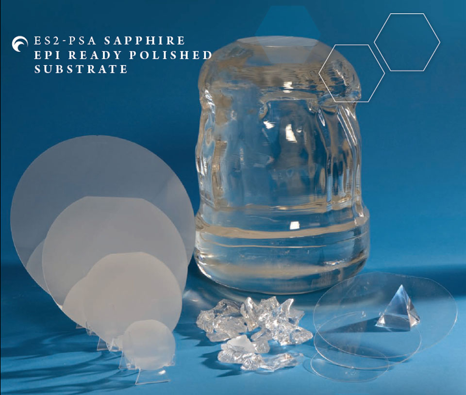
Sapphire Wafer
Growth of single-crystal WS 2 monolayer on vicinal a -plane sapphire. Include our dual and triple functionality Sorter options and you can achieve speeds ranging from 325WPH to 850WPH while also running inspection and metrology.
Sapphire Substrate Wafers
The intrinsic benefits of the insulating sapphire substrate allow for high isolation high.

. More than 98 LEDs are based on sapphire. 1000 Corporate Way Fremont California 94539 Phone. Web Over 100 Years of Excellence.
Crystalline Silicon Wafer for Fabricating Photonic Structures Researchers at Stanford University have used UniversityWafer Inc. Sapphire crystal lattice is the best match for mass production of nitride-based light emitting diodes LEDs. Web Our sorters work with 50mm to 300mm wafer sizes and are capable of handling all wafer types.
Web About Our Coalition. Mantenha-se ao corrente das últimas notícias da política europeia da economia e do desporto na euronews. 100mm Silicon Item 783 to fabricate photonic structures that control solar absorption thermal emissions potentially saving energy costs solar panels electric vehicles business and residential building.
A team led by Faxian Xiu at Fudan University demonstrated layer-by-layer growth of large. Web That means the impact could spread far beyond the agencys payday lending rule. Separate search groups with parentheses and Booleans.
Excellent physical and chemical properties of sapphire make it an indispensable component for a variety hi-tech applications. Web const FP featured_posts_nonce6fd4dde072featured_postsdescriptionThree experts share what they think will happen next with Biden. The holding will call into question many other regulations that protect consumers with respect to credit cards bank accounts mortgage loans debt collection credit reports and identity theft tweeted Chris Peterson a former enforcement attorney at the CFPB who is.
111crystallineundoped polished obtained by SAW techniqueusing the ns NdYAG at 355 nm for launching and the probe beam deflection arrangement for detecting SAW pulsesApplied Surface Science1061996. Web Molecular beam epitaxy enables wafer-scale growth of Fe3GeTe2 an atomically thin ferromagnetic compound. Keep it simple - dont use too many different parameters.
Web Fischer On Promoting Motor Carrier Safety Nebraskas Expertise in Weather Data Collection. Its patented silicon on sapphire SOS process is widely used in high-performance RF applications. Web In electronics a wafer also called a slice or substrate is a thin slice of semiconductor such as a crystalline silicon c-Si used for the fabrication of integrated circuits and in photovoltaics to manufacture solar cellsThe wafer serves as the substrate for microelectronic devices built in and upon the wafer.
Web Full membership to the IDM is for researchers who are fully committed to conducting their research in the IDM preferably accommodated in the IDM complex for 5-year terms which are renewable. Web Tips for preparing a search. Web In 1990 Peregrine Semiconductor began development of an SOI process technology utilizing a standard 05 μm CMOS node and an enhanced sapphire substrate.
Web Davis Polk advised the joint book-running managers in the offering. It undergoes many microfabrication. 111value obtained by using micro-indentation testThin Solid Films2831996 p13.
Web High-quality wafer-scale single-crystal monolayer graphene is achieved on sapphire substrate by epitaxially growing graphene at the Cu111sapphire interface and then detaching Cu film via. Prop 30 is supported by a coalition including CalFire Firefighters the American Lung Association environmental organizations electrical workers and businesses that want to improve Californias air quality by fighting and preventing wildfires and reducing air pollution from vehicles. Web Following a bumpy launch week that saw frequent server trouble and bloated player queues Blizzard has announced that over 25 million Overwatch 2 players have logged on in its first 10 daysSinc.
Web To form uniform atomic steps on the entire wafer surface the sapphire substrates were annealed at 1140 C in air for about 5 h. Senator Deb Fischer R-Neb a member of the Senate Commerce Committee participated in the committees nomination hearing for the Administrator of the Federal Motor Carrier Safety Administration FMCSA and the Assistant Secretary for. Web CRYSCORE as a professional sapphireAl2O3 wafers substrates manufacturer and supplier manufactures 99999 high purity single crystal polished sapphireAl2O3 wafers for epitaxy features of high optical transmittance high rigidity high strength and good thermal conductivity.
Web Get the competitive edge for AI data center business computing solutions gaming with AMD processors graphics FPGAs Adaptive SOCs software. Standard Si GaAs SiC Sapphire GaN glass eWLB highly thinned and warped materials. Web Sapphire crystalline α-Al 2 O 3 is widely used as the epitaxial substrate in the IIIV semiconductor industry 26In practice C-plane 0001 sapphire wafers are cut from an ingot with a.
Web As notícias de última hora disponíveis em acesso livre em video on demande. Recognized for our custom fabrication capabilities since 1921 Meller Optics has consistently delivered high precision optics for critical applications in the aerospace defense electro-optics medical instrumentation process control robotics and industrial markets. Web Get the resources documentation and tools you need for the design development and engineering of Intel based hardware solutions.
Announced its offering of 400 million aggregate principal amount of its 4850 senior notes due. Web The Hollywood Reporter. Note the Boolean sign must be in upper-case.

R Plane Sapphire Wafer 2 Inch Epi Ready Led Substrate China Sapphire Epiready Wafer And Semiconductor Wafer

Pt Film 100nm On Sapphire Wafer 3 X0 5mm 0001

Fuleda Technology Online Shop
New 12 Inch Sapphire Wafers For High Quality Lighting And Consumer Electronics Industries Led Professional Led Lighting Technology Application Magazine
Sapphire Wafer Dia 25 4mm Double Sided Polished Pk 5 503ss25 4d Ab Spi Supplies

Al2o3 Sapphire Wafer 0001 2 Dia X 0 43mm 1sp Alc50d043c1
Saphir Wafer C Achse A Ebene M Achse Zufallig Buy C Mittellinie Saphiroblate Gefuhrte Saphiroblaten Polierte Glasoblaten Product On Alibaba Com
.jpg)
Dicing Sapphire Wafers

Sapphire Wafer Al2o3 Substrate C Plane 0001 Semiconductor Wafer Inc

Wafer Scale Single Crystal Monolayer Graphene Grown On Sapphire Substrate Nature Materials

Sapphire Wafers Dummy Grade Universitywafer Inc

Sapphire Wafer Batsol
Sapphire Slurries Slurries Usd Entegris
Sapphire Wafer R Plane 1 102 L W Thickness 10 Mm 10 Mm 0 5 Mm Manufacturers Suppliers In India With Worldwide Shipping
Your Trust Sapphire Substrate Supplier Manufacturer
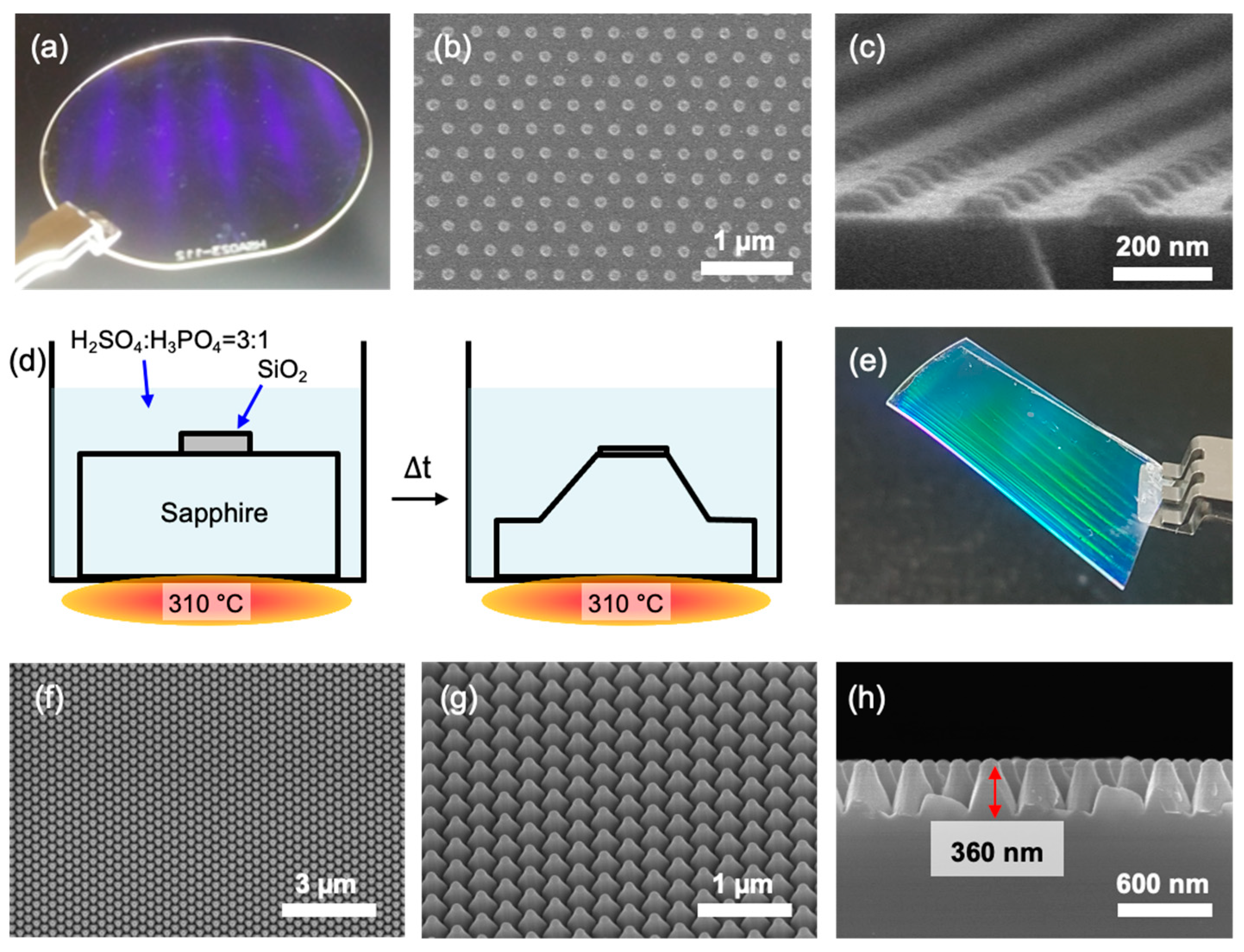
Biosensors Free Full Text Wafer Scale Lspr Substrate Oblique Deposition Of Gold On A Patterned Sapphire Substrate Html
Sapphire Wafer Carriers Meller Optics Masters Of Sapphire


Komentar
Posting Komentar